Altium Designer is a rules-driven board design environment, in which you can define many types of design rules to ensure the integrity of your board. Typically, you set up the design rules at the start of the design process and then verify that the design complies with the rules as you work through the design, and at the end of the design process.
Earlier in the tutorial we examined the routing design rules and added a new width constraint rule. We also noted that there were already a number of rules that had been created by the PCB Board Wizard, and that there were some existing design rule violations against these default rules.
Altium Designer
PCB设计支持多级设计规则约束功能。用户可以对同一个对象类设置多个规则,每条规则还可以限定约束对象的范围。规则优先级定义服从规则的先后次序。
为了校正电路板使之符合设计规则的要求,用户可以利用设计规则检查功能(DRC):
1.选择 Design»Board Layers & Colors (快捷按键: L) 并确认复选项 Show 及 System Colors 区的DRC错误标记选项已被选取,这样DRC错误标记将被显示。
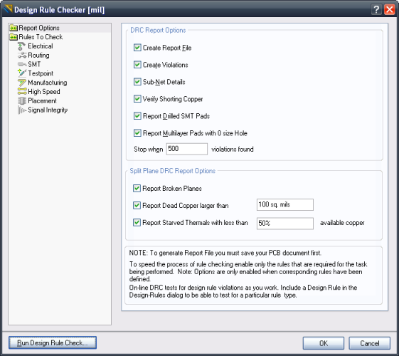
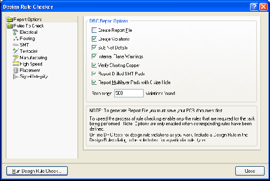
2.选择 Tools»Design Rule Check (快捷按键: T, D),打开 Design Rule Checker 对话窗口,使能 online 和 batch DRC 选项。
规则检测,Online和Batch均可以手工配置.
3.鼠标点击窗口左边的 Report Options 图标,保留缺省状态下 Report Options 区域的所有选项,并执行 Run Design Rule Check 命令按钮,随之将出现设计规则检测报告。并将同时弹出一个消息窗口。
4.点击违例条款 Silkscreen over Component Pads ,用户将跳转到相应违例报告区域。
5.点击违例条款 Silkscreen over Component Pads 的任一条记录,用户将跳转到PCB,并放大显示出现违例的设计区域。注意,放大的倍数取决于在 System - Navigation 环境配置内的设置。
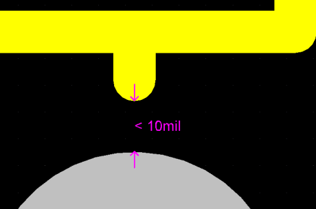 显示每项违例的细节,本例的丝印与焊盘的间隔少于10mil.
6.显示每项违例的细节, 如上图所示。注意用户可以通过 View Configurations 窗口内的 DRC Detail Markers 配置违例的图形显示颜色。
7.需要找出所有实际违反丝印与焊盘间安全间距规则约束的对象,可以选择菜单 Reports»Measure Primitives 命令。注意,用户可以通过快捷功能按键 CTRL+G 修改电气栅格的值。如5mil。
8.To resolve this error we can either modify the footprint, increasing the separation, or we can edit the design rule, decreasing the required separation. For this tutorial we will edit the design rule, to do this select Design»Rules from the menus to open the PCB Rules and Constraints Editor dialog.
9.In the Manufacturing category, open the Silkscreen Over Component Pads rule type, and click on the existing rule.
10.Edit the Silkscreen Over Exposed Component Pads Clearance value, changing it from 10mil to 9mil.
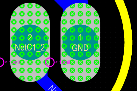
These pads are closer than the 13mil specified in the Clearance Constraint design rule.
* 运用习惯上与检查晶体管上焊盘间的安全间距相同的技术,检查阻焊数据与焊盘之间的间隙。
Switch back to the PCB document and you will see that the transistor pads are highlighted in green, indicating a design rule violation.
1.Look through the errors list in the Messages panel. It lists any violations that occur in the PCB design. Notice that there are four violations listed under the Clearance Constraint rule. The details show that the pads of transistors Q1 and Q2 violate the 13mil clearance rule.
2.Double-click on an error in the Messages panel to jump to its location on the PCB.
Normally you would set up the clearance constraint rules before laying out your board, taking account of routing technologies and the physical properties of the devices. Let's analyze the error then review the current clearance design rules and decide how to resolve this situation.
3.Open the PCB Rules and Constraints Editor dialog (Design»Rules). Expand the Electrical, then the Clearance rule type. There will be one Clearance design rule, click on it to display its settings.
4.Note that this rule requires All objects to be away from All other objects, at least 13mil. Since the clearance between the transistor pads is less than this, they generate a violation when we run a DRC.
5.We know that the minimum distance between the transistor pads is just over 10mil, so let's set up a design rule that allows the clearance constraint of 10mil for the transistors only.
6.Select the Clearance type rule in the Design Rules folder on the left of the dialog, right-click on it, then select New Rule to add a new clearance constraint rule.
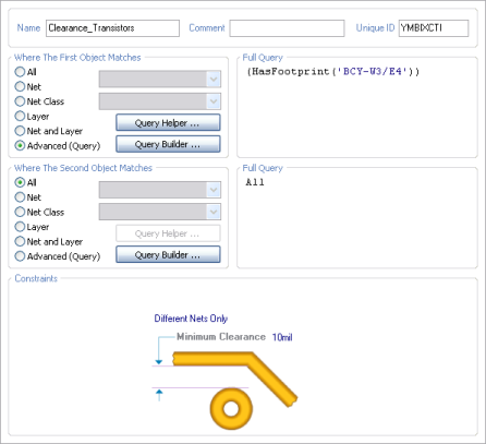
7.Click on the new Clearance rule, Clearance_1. Change the Name to Clearance_Transistors, and set the Minimum Clearance to 10mil in the Constraints section.
8.The final task is to set the Scope, or Full Query for the rule. There are a number of ways the rule could be scoped, the most appropriate in this case would be to target the rule to any component that uses the transistor footprint. To do that, select the Advanced (Query) option (in the upper section of the dialog), then click the *Query Builder button to open the Building Query from Board dialog.
9.Click Condition/Type Operator dropdown to Add first condition, and select Associated with Footprint from the list.
10.Set the Condition Value to BCY-W3/E4 (the footprint type being used by the transistor), then click OK to close the dialog. The new design rule should look like the figure shown below.
Design rule to set the clearance for all components using a specific footprint.
11.Click OK to close the PCB Rules and Constraint Editor dialog. The online DRC will run automatically, clearing the errors.
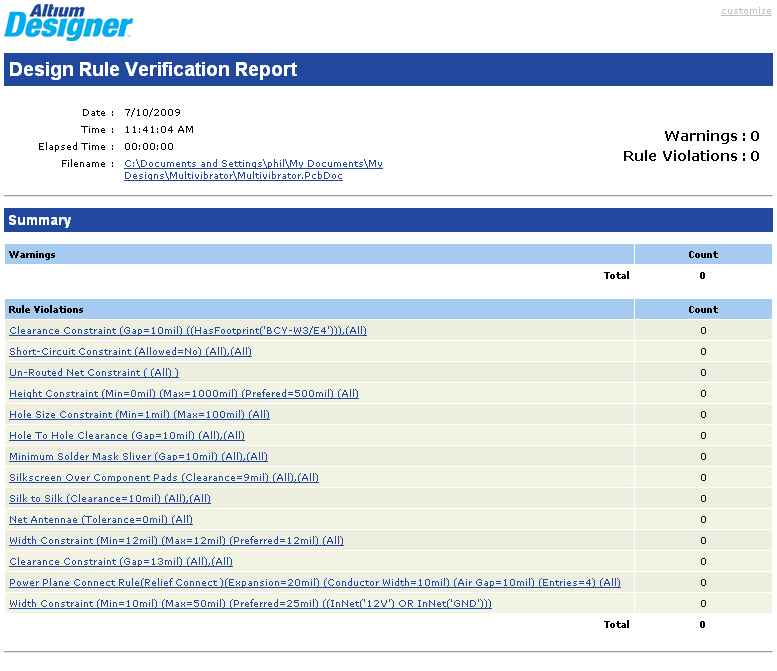
12.To confirm that the transistor pad clearance violations have been resolved, run the batch design rule check again (Tools»Design Rule Check). When the report opens scroll down and confirm that there are no violations.
一份清晰的DRC报告,显示了所有被判定了的违反规则的设计.
现在,用户就完成了PCB版图的设计,然后可以开始产生输出数据文档。不过,在产生输出制造数据之前,用户还可以利用Altium Designer的三维视图功能查看自己设计的PCB板。
在3D模式下查看电路板设计
现在,您的电路板设计已经基本完成,是时候研究一下它的3D模式了。3D模式,可以让您从任何角度观察您设计的板。要在PCB编辑器中切换到3D,只需选择View>>Switch To 3D [快捷键: 3]或者从列表中的PCB标准工具栏中选择一个3D视图配置。
Altium Designer软件的3D环境的要求支持是DirectX及相关技术,并使用一个兼容块独立的显卡。对于如何测试您的系统,以及让Altium Designer可以使用DirectX,打开Preferences对话框中的PCB Editor - Display (Tools>>Preferences)。
图30 3D旋转展示图
您可以滑动变换大小来看,旋转,甚至在板中间看,只要您使用如下操作:
缩放——按Ctrl+鼠标右拖,或者Ctrl+鼠标滚轮,或者PAGE UP / PAGE DOWN键。
平移——鼠标滚轮向上/向下,SHIFT+鼠标滚轮向左/右或向右拖动鼠标来向任何方向移动。
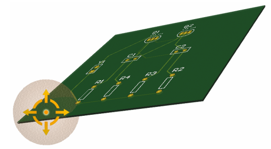
旋转——按住SHIFT键进入3D旋转模式。光标处以一个定向圆盘的方式来表示(图11)。该模型的旋转运动是基于圆心的,使用以下方式控制:
用鼠标右拖曳圆盘Center Dot,任意方向旋转视图。
用鼠标右拖曳圆盘Horizontal Arrow,关于Y轴旋转视图。
用鼠标右拖曳圆盘Vertical Arrow,关于X轴旋转视图。
用鼠标右拖曳圆盘Circle Segment,在Y-plane中旋转视图。
您可以使用View Configurations对话框[快捷键: L]来设定3D工作区的显示选项。可以选择各种表面和工作区的颜色以及垂直尺度,这样可以得心应手的来检查PCB的内部。一些表面有一种不透明的设置——越大的透明度的值越大,越少表示的光通过表面的光强度越小,使物体背面后面不明显。您也可以选择显示3D物体本身或者以2D层的颜色来着色该3D对象。
您可以将3D STEP格式模型导入到元器件的封装和PCB设计中并创建自己的3D物体。您也可以以STEP和DWG / DXF格式来输出PCB文件,以便运用到用于其他程序中。3D Vviewer可以导入VRML 1.0/IGES/STEP格式的3D物件,也可以导出IGES和STEP格式的3D物件。
注:任何时候在3D模式下,您可以以各种分辨率创建实时"快照(snapshots)",使用CTRL + C复制,这样就可以将图像(Bitmap格式)存储在Windows剪贴板中,用于其他应用程序。
为元器件封装创建和导入3D实体
到目前为止,我们已经到了最终PCB数据的核实查和输出阶段。Altium Designer软件的3D环境提供了一个逼真的优良的供视图查看及检查PCB组装的环境条件,是一个逼真的环境。
元器件封装本身存储有3D模型,用于在3D环境下渲染该元件。此外,精确的元器件间隙检查、甚至是装配整个PCB和外部的自由浮动的3D机械物体外壳都是可能的。这将用到机械CAD软件包,创建一个设计一体化的新的水平,这些Altium Designer软件正好可以提供。
如需要为元器件创建3D实体的详细资讯,请查找Creating Library Components教程中的3D元器件详细部分。
如需用MCAD软件进行3D实体一体化设计的更多信息,请查找 Integrating MCAD Objects and PCB Designs教程。
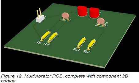
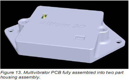
在 Integrating MCAD Objects and PCB Designs教程中,我们设计的板已经通过器件的3D模型完成了(图31)。教程将用机械外壳来装起整块板(图32)。板和元器件可以在Altium Designer软件安装中的 Examples/Tutorials/multivibrator_step文件夹中找到。
图31 3D效果图
图32 .装配效果图
检验PCB板设计
Altium Designer提供了一个规则驱动设计环境,在这里能够设计PCB,并且允许我们定义很多类型的设计规则来保证我们的PCB设计的完整性。典型地,我们在设计过程开始时建立设计规则,再在设计过程结束后用这些规则来校验修正设计标准。
在较早的教程指南中,我们检查了布线设计的规则和增添了一个新的宽度约束规则。我们还注意到,已经有一些由PCB Board EizardWizard创建的规则。
为了核实已经布好的电路板遵守设计规则,我们来执行设计规则检查(DRC):
1.选择Design>>Board Layers & Colors(快捷键:L),保证在System Colors部分中的DRC Error Markers选项中的Show按钮已经使能(打钩),以保证显示DRC错误标记。
2.选择Tools - Design Rule Check(快捷键:T,D)。保证在Design Rule Checker对话框的实时和批处理设计规则检测都被配置好。在其中一个各类上单击,比如:Electrical,可以看到属于那个种类的所有规则。
3.保持所有选项为默认值,点击Run Design Rule Check按钮。DRC就开始运行,报告文件Multivibrator.DRC就打开了。错误结果也会显示在信息面板。点击进入PCB文件,我们将会看到,该晶体管的焊盘是以绿色突出显示的,显示违反设计规则。
4.通过在信息面板中看错误报告清单,它列出发生在PCB设计的任何违反规则行为。注意有四种列出在清除约束规则中的违反规则。细节表明,晶体管Q1和Q2违反13mil的最小安全距离规则。
图33保持所有选项为默认值
1.双击Messages面板中的错误,可以跳到对应的PCB中的位置。
通常,我们会在布线之前,设置我们的安全距离规则,同时考虑到布线技术和设备的物理性能。让我们分析错误,然后再次检查现行的安全距离设计规则和决定如何解决这种情况。
图34错误信息
为了找出两个晶体管焊盘间的真实最小安全距离,有以下步骤:
1.选中PCB文件,光标定位于一个晶体管,按下PAGE UP键来放大视图影像。
2.选择Reports - Measure Primitives(快捷键:R,P)。光标将变成十字形字准线。
3.使光标定位于晶体管左边的焊盘中间,并点击或按下ENTER 。因为光标是超过两焊盘和连接它的布线,一个菜单会弹出让用户选择所需的对象。从弹出式菜单中选择晶体管的焊盘。
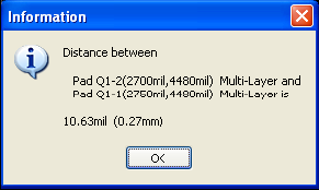
4.再一次,使光标定位于晶体管中间,并点击或按下ENTER 。从弹出式菜单中选择晶体管的焊盘。一个显示最小距离的信息框打开了,显示两个焊盘边缘的最小距离是10.63mil 。
5.关闭信息对话框,右键单击或按下ESC退出测量模式,然后使用V 、F的快捷键,重新缩放文件。
让我们看看当前的安全距离设计规则:
1.从菜单中选择Design - Rules (快捷键:D,R)来打开PCB Rules and Constraints Editor对话框。双击Electrical种类,在右边的对话框显示所有的电气规则。双击该安全距离类型,然后按一下就安全距离规则点击"Clearance"规则一项来以打开它。该对话框底部的区域将包含一个单一的规则,标明整个PCB板的最小安全距离为13mil 。晶体管之间的焊盘的距离小于安全距离,这就是为什么当我们运行DRC的时候,它们出现了违反规则的信息。
我们现在知道两个晶体管之间的最小焊盘距离是10mil多一点,让我们建立了一个只为晶体管的设计规则,大小为10 mil。
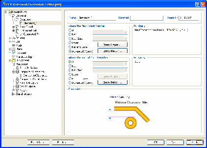
1.在设计规则文件夹中,选择安全间隙类型,点击右键并选择新规则添加一个新的安全间隙约束规则。
2.点击新的安全间隙规则,Clearance_1。在resulting页面中的Constraints章节中,设置Minimum Clearance为10 mil。
3.点击Advanced (Query),再点击Query Helper从Memberships Checks去建立条件检索,或者也可以为第一个对象(图35)在接下来的条件检索中打印进去。
HasFootprintPad('TO-92A','*')
那个星号表明在封装里名为"TO-92A"的任何焊盘。
1.保持第二个对象范围为ALL,并单击OK。单击Apply,然后点击OK以关闭PCB Rules and Constraints Editor对话框。
2.现在,我们可以从设计规则检测对话框(Tools - Design Rule Check)按一下运行设计规则检查按钮。重新运行DRC,不会有违反规则的行为。
3.保存已经完成的PCB和工程文件。
图35 使用PCB规则系统规定参数编辑器对话框创建规则。
恭喜,用户已经完成了PCB的布局布线,准备生成输出文件。
深圳宏力捷推荐服务:PCB设计打样 | PCB抄板打样 | PCB打样&批量生产 | PCBA代工代料